05b · Field monitors: where they sit, what they record
Every simulation example so far showed a field map, always from the default monitor. This notebook is about controlling that monitor:
each axis in
spec.field_monitorsadds one plane normal to it —"z"is the top view,"y"the side view,"x"the cross-section;by default a plane sits at the domain center along its normal (
x/y), or at the average mid-plane of the device layers (z);spec.field_monitor_positionspins a plane at an absolute coordinate, andspec.field_monitor_wavelengthspicks what it records;plot_monitor_planes(solver)shows all of it before anything runs.
The device is the Si→SiN escalator from the cookbook — light enters in a silicon core and couples upward into a nitride core 300 nm above it. A device whose action happens in the vertical plane is exactly where monitor placement starts to matter.
from pathlib import Path

import matplotlib.pyplot as plt
import numpy as np

from gds_fdtd import SimulationSpec, Technology, get_solver
from gds_fdtd.lyprocessor import load_cell
from gds_fdtd.plotting import (
    component_outlines,
    plot_field,
    plot_monitor_planes,
    port_plane_outlines,
)
from gds_fdtd.simprocessor import load_component_from_tech


def _find(rel: str) -> Path:
    for base in (Path.cwd(), *Path.cwd().parents):
        if (base / rel).exists():
            return base / rel
    raise FileNotFoundError(rel)


REC = _find("examples/05_fields_and_modes/recorded")

tech = Technology.from_yaml(_find("examples/tech.yaml"))
cell, layout = load_cell(str(_find("examples/10_cookbook/si_sin_escalator.gds")),
                         top_cell="si_sin_escalator")
comp = load_component_from_tech(cell=cell, tech=tech)
print(f"{comp.name}: {comp.bounds.x_span:.1f} x {comp.bounds.y_span:.1f} um, "
      f"ports {[p.name for p in comp.ports]}")
00:26:15 PDT WARNING: Using canonical configuration directory at
             '/home/mustafa/.config/tidy3d'. Found legacy directory at
             '~/.tidy3d', which will be ignored. Remove it manually or run
             'tidy3d config migrate --delete-legacy' to clean up.
si_sin_escalator: 18.0 x 3.8 um, ports ['opt1', 'opt2']
1 · The default monitor lands between the cores
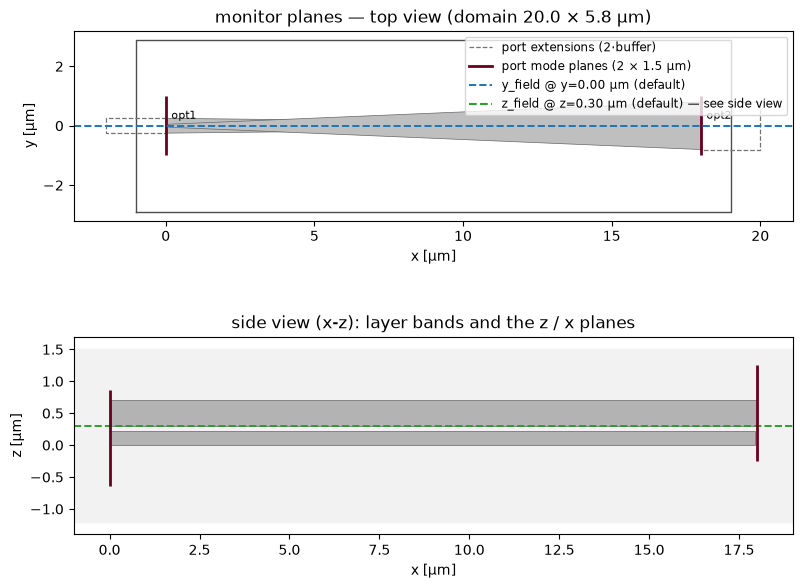
The escalator has two device layers: Si at z = 0–0.22 µm and SiN at
z = 0.3–0.7 µm. The default z-plane is the average of the layer mid-planes
— (0.11 + 0.5)/2 ≈ 0.3 µm — which here falls in the gap between the two
cores, where neither mode is strongest. plot_monitor_planes makes that
visible on the constructed solver (offline, nothing runs):
spec_default = SimulationSpec(
    wavelength_start=1.5, wavelength_end=1.6, wavelength_points=11,
    mesh=10, z_min=-1.2, z_max=1.5, field_monitors=("y", "z"),
)
solver_default = get_solver("tidy3d")(comp, technology=tech, spec=spec_default)
plot_monitor_planes(solver_default)
plt.show()
2 · Pin the plane where you want it
field_monitor_positions takes absolute coordinates (µm) per axis. Here the
z-plane goes to 0.11 µm — the middle of the Si core — so the top view
shows the light where it is launched. The side (y-normal) plane keeps its
default: the domain’s y-center, which is where the waveguide runs.
field_monitor_wavelengths=(1.55,) records a single wavelength instead of
the whole 11-point spectrum, which keeps the downloaded field data small:
spec = SimulationSpec(
    wavelength_start=1.5, wavelength_end=1.6, wavelength_points=11,
    mesh=10, z_min=-1.2, z_max=1.5,
    field_monitors=("y", "z"),
    field_monitor_positions={"z": 0.11},
    field_monitor_wavelengths=(1.55,),
)
solver = get_solver("tidy3d")(comp, technology=tech, spec=spec)
plot_monitor_planes(solver)
plt.show()
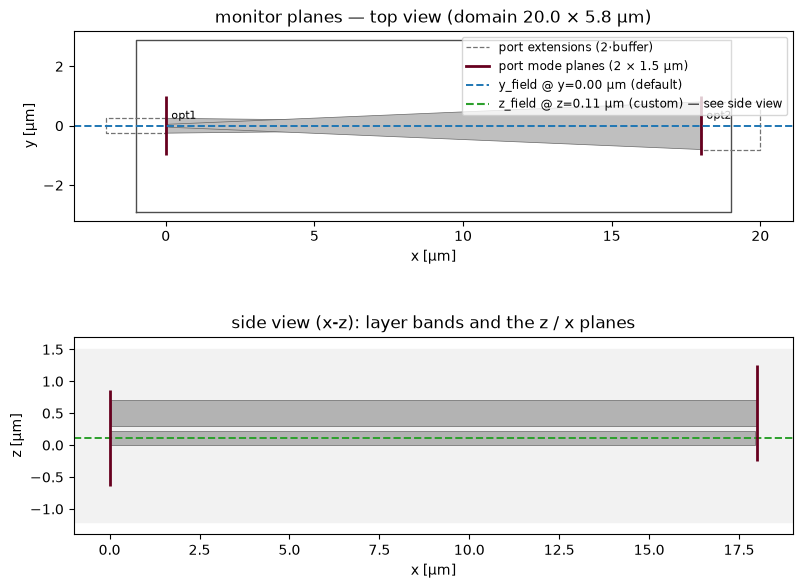
The z-plane label switched from (default) at 0.30 µm to (custom) at 0.11 µm, inside the Si band of the side view.
The same solver renders as an interactive 3D scene — the two cores, the translucent cladding, the port cones, the wireframe domain, and both monitor planes, orbitable and clickable:
from gds_fdtd.viewer3d import show_3d  # noqa: E402

show_3d(solver, height=460)
3 · The side view: light climbing the stack
This spec ran on tidy3d (~0.05 FC; artifacts in recorded/, see
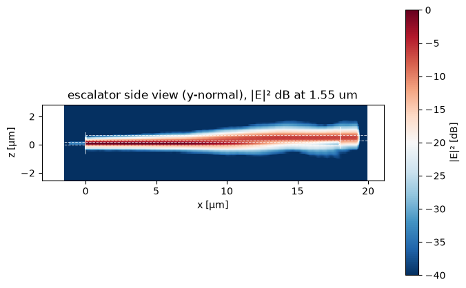
PROVENANCE.md). The y-normal monitor cuts along the propagation axis, so
it shows the vertical story: the mode enters in the Si core (z ≈ 0.1 µm),
transfers upward through the taper, and exits in the SiN core (z ≈ 0.5 µm).
The dashed outlines are the layer bands and port-extension stubs
(component_outlines), and the short vertical strokes at the ends are each
port’s mode plane at its real depth (port_plane_outlines):
fy = np.load(REC / "escalator_field_y.npz")
plot_field(
    fy["mag2"][0], x=fy["h"], y=fy["v"], scale="db",
    outline=component_outlines(comp, axis="y", buffer=2 * spec.buffer)
    + port_plane_outlines(comp, spec, axis="y"),
    title=f"escalator side view (y-normal), |E|² dB at {fy['wavelength_um'][0]:.2f} um",
)
plt.ylabel("z [µm]")
plt.show()
4 · The pinned top view: light leaving its own plane
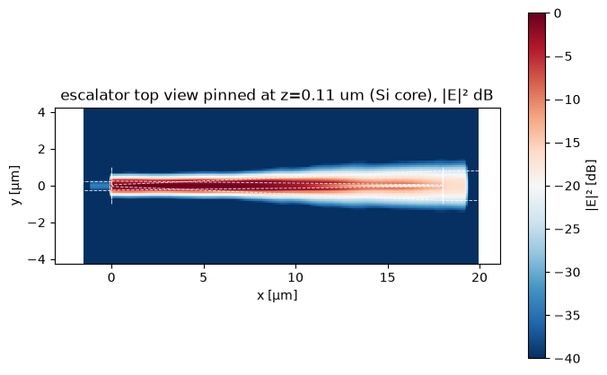
The z-plane at the Si core tells the same story from above: strong field in the input waveguide, then the intensity fades out along the taper — not because light is lost, but because it moved up and out of this plane into the nitride. (Re-pin the monitor at z = 0.5 µm and the picture inverts.)
fz = np.load(REC / "escalator_field_z.npz")
plot_field(
    fz["mag2"][0], x=fz["h"], y=fz["v"], scale="db",
    outline=component_outlines(comp, axis="z", buffer=2 * spec.buffer)
    + port_plane_outlines(comp, spec, axis="z"),
    title="escalator top view pinned at z=0.11 um (Si core), |E|² dB",
)
plt.show()
5 · The numbers behind the pictures
The same run produced the S-matrix; the escalator transfers the band with low loss, confirming the field pictures:
from gds_fdtd.smatrix import SMatrix  # noqa: E402

sm = SMatrix.from_npz(REC / "escalator_tidy3d.npz")
thru = sm.sel(sm.port_names[1], sm.port_names[0], 1, 1)
il_db = 10 * np.log10(np.abs(thru) ** 2)
print(f"through-path insertion loss: {il_db.min():.2f} .. {il_db.max():.2f} dB "
      f"across {sm.wavelength_um.min():.2f}-{sm.wavelength_um.max():.2f} um")
through-path insertion loss: -0.07 .. -0.06 dB across 1.50-1.60 um
Recap
One monitor plane per axis in
spec.field_monitors; defaults are the domain center (x/y) and the device layers’ average mid-plane (z).spec.field_monitor_positionspins any plane at an absolute coordinate — for multi-layer stacks the default z-plane can sit between the layers, so pin it to the core you care about.spec.field_monitor_wavelengthsrestricts what is recorded; the S-matrix keeps its full spectral resolution independently.plot_monitor_planes(solver)shows every plane, labelled default/custom, before you spend anything.
11_bragg_grating uses the wavelength knob on a strongly dispersive device:
the same monitor, in and out of a Bragg stopband.